How to Design a PCB Layout?
There are so many softwares by which we can make layouts such as KiCad, OrCAD, eagle, spice etc. Here we will discuss about KiCad and we are going to use it for making layout.
Here is the small introduction about
KiCad, its much user friendly and its little bit easy to understand too. In KiCad we have to follow total 4 steps to complete layout of pcb. These steps are as shown in picture.
For brief details of KiCad, just google it!
1. EESchema (schematic editor)–
In this step we have to draw the schematic for required circuit.
2. CVpcb (components to modules)-
This step shows how to assign footprints to a particular component.
3. PCBnew (PCB editor)-
Here actually you have to draw the tracks according to your wiring made in EESchema.
The width of track can be adjusted according to our requirement.
4. GerbView (Gerber Viewer)-
To send your board to a manufacturer you will need to generate a gerber file.
Fig. 1: Image showing Icons of Various Components of KIcad
See for the Downloads to start at the end.
Starting a new project
First of all we have to create our
project file in which we will work. E.g. demo. For that click on file>new>demo and hit enter. Then demo.pro file will be created. That “.pro” extension to the file indicates it’s a project file.
Fig. 2: Screenshot of Creating New Project in KIcad
After creating the new project we have to click the 1st icon EESchema which is shown in Fig. 1
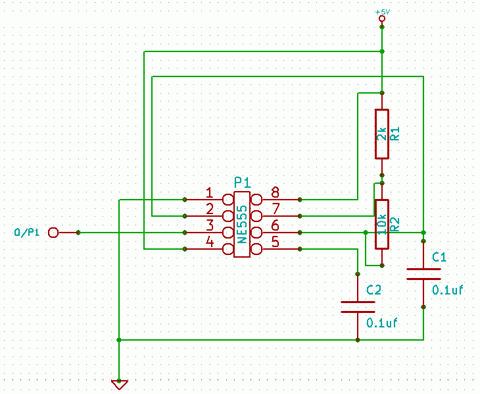
Circuit Diagram-

Fig. 3: Circuit Diagram of a 555 IC based Project
Step1: EESchema of How to Design a PCB Layout?
Now click on the EESchema i.e. 1st icon. The new window will pop up to draw the schematic of any circuit. We have one sample circuit diagram taken from the web as above.
It will show some error like demo.sch (in above case) not found. Ignore it and click OK. Here “.sch” extension indicates its schematic file. New window will look like below. Now zoom it in and we will get the grids where we have to draw our schematic.
Save the schematic. Make page setting and put the title for schematic. You may give anything you want.
To draw the schematic we have to place components on the given sheet. For that click on place> component. The component window will appear. In that you can select components from the list. Even to put resistor you may simply write “R” and click on search keyword. Double click on that component and it will be placed on the sheet. You may brows the category view for the components. If there are some devices/components are missing then try to add library files into Your drive in which KiCad is installed:KiCadsharelibrary. So you must have to copy those libraries into library folder. You can download libraries by searching them on google like NE555 KiCad library. According to your circuit diagram make the schematic.
Put cursor on the component and right click on same. From that list you may delete, edit, move and rotate the component according to your requirement. Likewise to select LED just simply search LED or you can put it from the list. After completing your schematic, save it.

Fig. 4: Screenshot of Saving a Schematic by EESchema in KIcad
After arranging components to the proper places it’s time to make them connected with the wire. Go to place> wire. Now you can connect more than 2 components with wire. If there is connection between 2 wires in circuit diagram, in schematic you will see the node (bubble) which shows there is connection. 1st step is almost complete here. If you want to add node then click on ‘place a junction’.
As you have done with schematic before going to assign footprints you have to give proper names to the components. As we have taken small sample for demo, if the schematic is much larger and contains lots of components, it’s difficult to provide proper names. Instead there is function to annotate the schematic automatically. If you can see icon indicating annotate schematic click on it. If you are using single sheet don’t change anything just click on annotation. Click OK button. You will see that your whole schematic is annotated!
To assign footprints we must create netlist. Prior to the annotation icon there is icon indicating netlist generation. This netlist can be used in PCBnew, OrCAD, spice etc. don’t change anything, click on netlist and save.
Now the schematic will look like below. Keep in mind that I have drawn it as in circuit diagram to make you clear. You can draw it according to you but make sure that the connections are accurate.
(Note- I have forgot to put power supply connection for +5V supply so you add it while drawing schematic)

Fig. 5: Image of a Schematic Drawn by EESchema in KIcad
Save your work. Close the current sheet. 1st step is done!
Step2: CvPCB of How to Design a PCB Layout?
In this step we have to assign footprints for respective components. It’s very easy for components like capacitor, resistor because we can bend their leads, but it’s very difficult if we going to assign it for any DIP/QFP/SMD ICs. As there is more or lesser distance between pins than actual distance between IC pins may cause our PCB useless. So care must be taken while assigning the footprints.
Let’s start with this step.
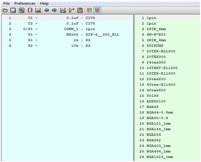
Open CvPCB. Click OK button as it will show some error. You will see all components which you have in your schematics. Now if you click on any component present at left column you will get filtered footprints list. Next to that you will get unfiltered footprints at right column. Click on any footprint and click on view selected footprint.
You can see the distance between 2 pins. For ease of calculation right click> grid select> 39.4 mils(1mm). It’s very useful for calculating distance between 2 pins. You can get 3D view of that footprint by clicking on the 3D button. Close that window, get suitable footprint for your component. After that double click on that footprint then it will be assigned to that respective component. We have our sample schematics so the assigned footprint will look like following figure.

Fig. 6: Screenshot of CvPCB in KIcad
Now click on create export file and click save. Don’t change name or anything.

Fig. 7: Screenshot of Creating Export File in CvPCB
You have done with 2nd step. Minimize or close the current window.
Step3: PCBnew
After opening PCBnew you will get zoomed out window. We have created netlist file, here we need to read that netlist file to draw tracks. Click on read netlist file and then click on read current netlist. Look at only Nelist Dialog window below not behind that.
Fig. 8: Screenshot of PCBnew in KIcad
One point to keep in mind that why I’m not showing you all icon is that you will get environmental with this software which is basic step to learn it.
Okay now your project will be at top-left side of sheet. Zoom it in. Now you have to move on sheet and place them separately as they gathered after opening window. For that see the following fig.
Fig. 9: Screenshot of Autoplacing Modules in PCBnew in KIcad
Select the components and right click on it. Then make above selection. Autoplace all modules will automatically place your modules in systematic manner. Now the hard step comes!
Concentrate on the connection between components. If you couldn’t see connections click on manual and automatic move or place of modules. After arranging components to suitable places it’s time to connect them with tracks. You can rotate the component if connection is getting complicated. For the 1st time you can copy the tracks and placing of components as I have done. While practicing you may choose your view. Click on add tracks and vias. Click on any pin of component and click on other pin which has connection with that pin. If you made connection, double click to fix that track.
Normally it’s better to keep track width of 1mm thick. As for learners for practice 1mm thick track width is enough. If you are going well with it then you may choose suitable track width. To change track width click on Design Rules and make changes to track width. Put suitable track width and click OK.
Fig. 10: Screenshot of Design Rules Editor in KIcad
ONE THING TO TAKE CARE THAT DON’T DRAW TRACKS WITH STRAIGHT LINES!!! THEY MUST BE DRAWN WITH 45degrees. THIS SOFTWARE WILL CUT THE LINE IN 45degrees ITSELF WHILE MOVING. JUST MAKE SURE THAT TRACKS ARE DRAWN WITH 45degrees AND WONT OVELAP WITH EACH OTHER. IF YOU TRY TO OVERLAP IT WILL NOT ACCEPTABLE BY SOFTWARE. IF THE DISTANCE IS VERY SHORT BETWEEN TWO CONNECTIONS, THAT TIME YOU MAY DRAW IT WITH STRAIGHT LINE. THE REASON BEHIND THAT WILL LET YOU KNOW LATER. AND YES WE ARE MAKING SINGLE LAYER PCB. THIS SOFTWARE SUPPORTS MULTIPLE LAYER PCB BUT WE WILL TRY SINGLE LAYER AT THIS TIME!
Fig. 11: Image showing Right and Wrong Methods of Creating a Net
After going through these instructions you will get to know how to draw exact tracks. I have drawn it so just go through it if you’re in trouble.

Fig. 12: Image of a PCB Layout Designed on KIcad
Here I have assigned footprint of 1 pin connector has much wider diameter. This is labeled as CONN_1. When you are going to assign footprint make sure that diameter is about 1-1.5mm or if you have 1 pin connector you may see the footprint of that. You can see 3D view of this pcb by clicking on 3D display tab. Then zoom window in and you will get 3D view.

Fig. 13: Screenshot of 3D Viewer in KIcad
Now it’s time to create GERBER file. Click on plot and in that select Gerber and click Plot. It will create Gerber file which many of organization send to manufacturers. It will create respective file and here we have done with 2nd last or maybe last step for some users.
Step4: GerbView
Why to create Gerber file? It’s because there are lots of software which are used to make layouts. I have told at start that OrCAD, KiCad, Eagle etc softwares are useful for making layouts. Fact is I use KiCad but many of manufacturers may use different software other than KiCad. So Gerber file is a file which will help manufacturer to know about your project and that manufacturer couldn’t make changes to the Gerber file. Now there are softwares which allow making changes to the Gerber file. Forget it we are just learner. We don’t have big budget project so it’s not mostly usable for individual. We can see gerber file by clicking on file>open and selecting any file which we have already created.
Manufacturer can see the following views like top view and bottom view

Fig. 14: Screenshot of Gerbview in KIcad
Fig. 15: Screenshot of Gerbview in KIcad
After making a layout it’s time to make PCB, but I think you knew how to make it. It’s already posted here by someone.
Downloads
Downloads-
.exe file is for windows and .tgz is for linux
Or search for particular library here
So friends this is just primary stage to make layout. In deep there are lots of functions like assigning custom footprint to any component if required is not available etc.

Related


